 n-1
xm. nwmk -------------------------------------------------------(1)
(draft)
Abstract : An
algorithm well suited for implementation on a FPGA is developed. The algorithm
distributes computation and memory requirements evenly among the processors.
The algorithm integrates the ram used on to the procesor itself to achieve
higher speed. It also reduces the width of the interconnections between
the different stages of FFT.
INTRODUCTION
Parallel pipelined FFT processors are employed to meet the growing demand of high processing rate. Highly parallel implementations obtain high computation rates but requires the simultanious distribution of all data samples. The high rate of distribution of data required to keep the processors busy is impossible to achive especially in real time applications involving word-serial data. This problem coupled with limited i/o resources in FPGAs makes the parallel algorithm inefficient.
The cascade FFT computes one transform in O(N) processing
cycles, producing the o/p sequentially at the input data rate. So the cascade
FFT is ideally suited for 1-dimensional real-time signal processing where
data arrival is word-serial in nature. But cascade FFT requires registers
organised as shift-registers between butterfly computation units with varying
depths from 2 to N/2 words. Jones and Sorenson proposed an algorithm for
overcoming this, in evaluating their multiprocessor architecture for FFT.
Yu Tai Ma proposed an algorithm to reduce the number of twiddle factors
in each processor to a minimum. These ideas with some modifications are
used to design a 32-point FFT processor using multiple FPGAs.
A PARALLEL FFT ALGORITHM
The DFT of N-point is defined as
Xk = m=0 n-1
xm. nwmk -------------------------------------------------------(1)
wnmk = exp(-j.2 /N
m.k)
k = 0,1,.......,N-1
N = 2n
N = N1.N2
m = N1m2 + m1
k = N2k1 + k2
N1 = 2n1
N2 = 2n2
m1,k1 = 0,1,2,3,...........,N1-1
m2,k2 = 0,1,2,3,...........,N2-1
Then eq.(1) can be expressed as
XN2k1 + k2 = m1=0 N1-1
( N1N2 Wm1(N2k1 + k2) ) m2=0
 N2-1
(x N1m2 + m1 . N2Wm2k2 ) --------(2)
eq.(2) can be further expressed as
YN1k2 + m1 = m2=0 N2-1
(x N1m2 + m1 . N2Wm2k2 )
XN2k1 + k2 = m1=0 N1-1
YN1k2 + m1 . ( N1N2 Wm1(N2k1 + k2) ) -------------------------(3)
eq.(3) can be computed easily through the FFT algorithm and (4) can be computed in a similar way as is the standard FFT algorithm. The flow for a 16-point FFT using such an algorithm is as shown in fig.(1).

Fig.1. Flow diagram for 16-point FFT

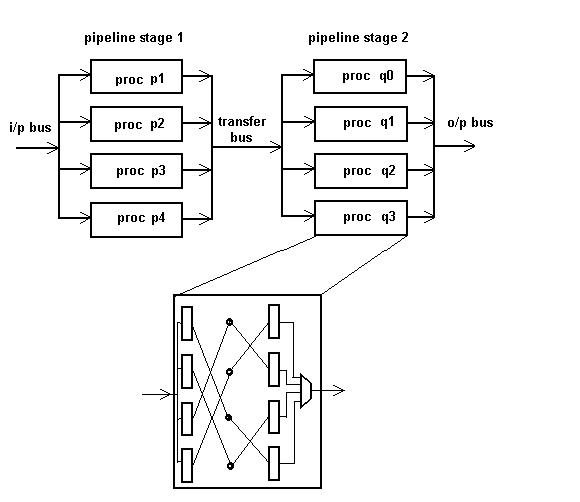
Fig.2 : Division of computations among the FPGAs
The division of computations among the FPGAs is as shown
in fig.2. There are 4 independent length-4 transforms in the first 2 stages
of the radix-2 decimation in time algorithm as the first part of FFT computation.
The last 2 stages of 4 independent length-4 transforms form the second
part.There are 4 processors at each pipeline stage and each FFT processor
computes a 4 point FFT. The reduced twiddle factor tables stored are shown
in table-I
Table 1 : REDUCED TWIDDLE FACTOR TABLES STORED IN FFT PROCESSORs at second pipeline stage.
| PROCESSOR NO. | 0 | 1 | 2 | 3 |
| 0
1 2 3
|
--
-- -- -- |
16W0
16W1 16W2 16W3 |
16W0
16W2 16W4 16W6 |
16W4
16W5 16W6 16W7 |
Processors
The processors used in the two pipeline stages incorporate both the twiddle factor ROM and the data RAM on the chip. The look-up table based logic in some of the commercial FPGAs makes this idea all the more efficient. Each processor is structured internally as shown in Fig.3. The single input and output buses in each processor is time shared between the different butterfly computation units for i/o of the samples and transforms.

Fig.3: Processor organisation and internal structure of
FFT processors.
There is a single input[x(m)], output[X(k)] and transfer[Y(N1k2+m1)] bus time-shared between the processors. To prevent contention of the bus, data transforms are done as in Fig.4.
|
X1 from
q2
y4 from p0 to q2 x0 to p0 |
X9 from
q2
y5 from p1 to q2 x1 to p1 |
X5 from
q2
y6 from p2 to q2 x2 to p2 |
X13 from
q2
y7 from p3 to q2 x3 to p3 |
|
X3 from
q3
y12 from p0 to q3 x4 to p0 |
X11 from
q3
y13 from p1 to q3 x5 to p1 |
X7 from
q3
y14 from p2 to q3 x6 to p2 |
X15 from
q3
y15 from p3 to q3 x7 to p3 |
|
X0 from
q0
y0 from p0 to q0 x8 to p0 |
X8 from
q0
y1 from p1 to q0 x9 to p1 |
X4 from
q0
y2 from p2 to q0 x10 to p2 |
X12 from
q0
y3 from p3 to q0 x11 to p3 |
|
X2 from
q1
y8 from p0 to q1 x12 to p0 |
X10 from
q1
y9 from p1 to q1 x13 to p1 |
X6 from
q1
y10 from p2 to q1 x14 to p2 |
X14 from
q1
y11 from p3 to q1 x15 to p3 |
A controller generating control signals for data transfers is used for write enables to input registers and for the mux select signals at the output of each processors. To reduce the number of control signal lines to be generated by the controller all the three tranfers, namely input, output and intermediate transefers are done with the same signals.
(incomplete)