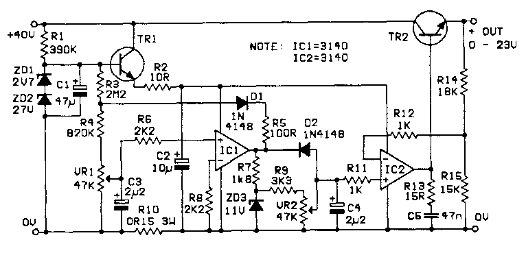
As I carry out a lot of repairs on C.B. and audio equipment, I need a variable power supply with very good current limiting and protection. The circuit I designed for this purpose is shown in the diagram below. This power unit will deliver a current from zero to about 4.25A at a voltage from zero to about 23V. With the component values shown, the short circuit protection is 400 mA, but it can be set below this figure; for instance, an LED can be connected directly to the power supply and the current adjusted to light it without destroying it. The unit is not difficult to build, and in my opinion it outperforms many commercial power supplies. Mine has been in use for more than a year, and has given no trouble at all in that time.
The first op-amp (IC1) acts as a comparator, comparing the voltage drop across R10 with that set by the wiper of VR1, derived from the Zener diodes ZD1 and ZD2. Two diodes are used in series instead of a single one because Zener diodes below 5V have a negative temperature coefficient. ZD2 has a positive temperature coefficient, so the two tend to cancel out and the reference voltage is more stable. The current available from the unit can be increased or decreased by adjusting VR1.
The output from IC1 is applied to VR2, and because it is constantly reacting to variations in the current through R10, ZD3 is placed in the circuit to provide a reference voltage for VR2. The second op-amp (IC2) compares the voltage at the junction of R14 and R15 with the voltage set by the wiper of VR2, and by varying this setting the output voltage can be increased or decreased.
Diodes Dl and D2 together with R5 provide "foldback" current limiting and in the event of a short circuit the current output is limited to about 400mA. If the output is short circuited, the voltage at the non-inverting input of IC2 would fall almost to zero and this would limit the base drive to Tr2. If the current through R10 rises to a point at which the voltage across it is about 70% of the reference voltage applied to the non-inverting input of IC1, the output of IC1 will swing below the voltage at the junction of R3 and R4. Dl then conducts through R5 and IC1; this reduces the reference voltage on its non-inverting input which in turn takes the output more negative until it is at ground potential, the circuit is stabilised and practically no current flows through R10.
If a large load were applied to the output, a very large current would flow through Tr2 and R10, which would burn out Tr2 if not quickly checked. If, for example, the voltage at the slider of VR2 was 1OV, the voltage across C4 would be equal to this. If a large current was flowing, IC2 would try to reduce the base drive to Tr2; it would also try to discharge C4, but could only do this through VR2, R7 and R9. This would take too long, and Tr2 would be destroyed. The presence of D2 allows C4 to discharge rapidly, so reducing the time for IC2 to shut down.
Trl should have a gain of at least 250. A BC182LB was used in the circuit, but any equivalent transistor of similar gain could be used. Tr2 must be a high power Darlington, preferably a T03 type mounted on an adequate heat sink. Either MJ1001 or MJ3001 would be suitable.